Six precision stages — from raw silicon feedstock to certified, ready-to-deploy solar components.
Manufacturing Stages
From Silicon to Sunlight
01
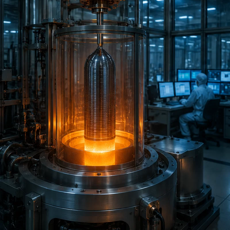
Ingot Growth
Silicon Crystal Growing
Polysilicon melted and Czochralski-pulled at 1,420°C. 40-hour controlled growth cycle with precise crystal orientation and resistivity management.
02
Wafer Slicing
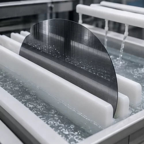
Diamond-Wire Cutting
Diamond-wire cut into ≤180μm wafers, cleaned in ultrapure water, EL-inspected, and sorted by resistivity grade for optimal downstream matching.
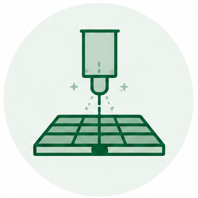
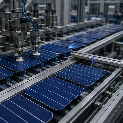
03
Cell Fabrication
TOPCon Processing
Texturisation, phosphorus diffusion, tunnel oxide deposition, PECVD AR coating, and silver/aluminium metallisation. Each cell flash-tested individually.
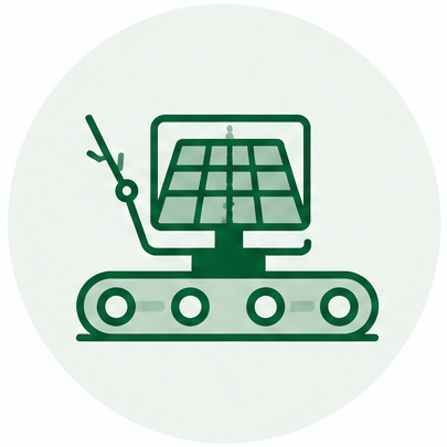
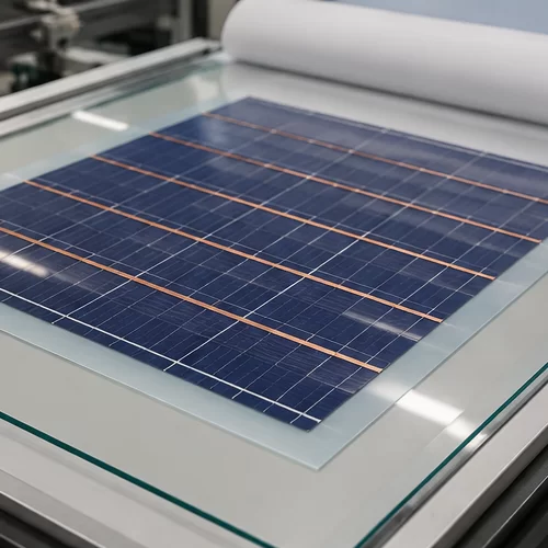
04
Module Assembly
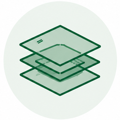
Lamination & Framing
Cells tabbed with bus bar ribbons, laid on low-iron glass with EVA encapsulant, vacuum-laminated, framed, and fitted with junction boxes.
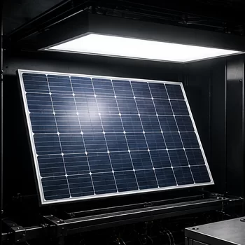
05
Quality Testing
IEC 61215 / 61730 Testing
Flash testing, EL imaging, thermal cycling (−40°C to +85°C × 200 cycles), damp-heat 1000hr, hail impact, and PID resistance verification.
06
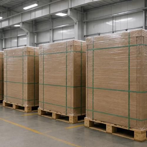
Dispatch
Certified Global Dispatch
Unique serial numbers, IEC 62759-compliant packaging, quality certificates, test reports, and performance warranty documentation with every order.
Manufacturing Stages
From Silicon to Sunlight
01
Ingot Growth
Silicon Crystal Growing
High-purity polysilicon is melted at approximately 1,420°C and transformed into mono-crystalline silicon ingots through the advanced Czochralski (CZ) crystal growth process. Automated thermal control systems ensure precise crystal orientation, uniform resistivity, and ultra-low impurity levels essential for high-efficiency N-Type TOPCon applications.
Ultra-pure polysilicon feedstock
Automated thermal profile control
Resistivity & orientation verified at every pull
1,420°C process
40-hr growth cycle
Czochralski method
02
Wafer Slicing
Diamond-Wire Cutting
Mono-crystalline ingots are precision sliced into ultra-thin wafers using advanced high-speed diamond-wire cutting technology. The wafers undergo ultrapure water cleaning, EL inspection, thickness calibration, and resistivity-based grading to ensure maximum downstream cell efficiency and manufacturing consistency.
Diamond-wire precision slicing technology
Minimal kerf loss for higher silicon utilization
Grade-matched resistivity sorting
≤130µm wafers
EL inspection
Ultrapure water wash
03
Cell Fabrication
TOPCon Processing
Wafers undergo advanced photovoltaic cell processing including texturisation, phosphorus diffusion, tunnel oxide passivation, PECVD coating, laser edge isolation, and precision silver/aluminium metallisation. Each cell is individually flash-tested to ensure superior conversion efficiency and long-term performance reliability.
Low LID & enhanced carrier lifetime
Advanced passivation layer formation
Superior low-light and high-temperature performance
25%+ cell efficiency
PECVD coating
Per-cell flash test
04
Module Assembly
Lamination & Framing
High-efficiency TOPCon cells are interconnected using precision Busbar & Ribbons and integrated with high transmission low-iron Solar Glass and Encapsulants. The modules undergo vacuum lamination, framing, curing, and junction box integration under automated production environments.
High-transmission low-iron glass
Advanced encapsulant bonding system
IP68 junction boxes & weatherproof seals
16BB high-density interconnection design
Vacuum lamination
Aluminium frame
05
Quality Testing
IEC 61215 / 61730 Testing
Every module undergoes rigorous multi-stage testing and reliability validation based on international IEC standards to ensure superior electrical performance, durability, and long-term operational stability under extreme environmental conditions.
Potential Induced Degradation (PID) testing
1,000-hour damp heat exposure testing
25 mm hail impact resistance verification
IEC 61215
IEC 61730 (Part-1 & Part-2)
200 thermal cycles(-40°C to +85°C)
06
Dispatch
Certified Global Dispatch
Each module is digitally traceable through unique serialisation and QR-based tracking systems, supported by quality certificates, test reports, and warranty documentation. Advanced packaging systems ensure safe global transportation and long-term product protection.
Unique serial number & QR traceability
Protective packaging
25-year linear performance warranty
Global logistics and shipment compliance
IEC 62759
Serial tracked
Full test reports
Quality First
Built to the Highest Standards
Every solar module compliant as per IEC 61215, IEC 61730, BIS, and ALMM requirements. Zero-defect policy across all manufacturing stages.
 3GW Solar Module Manufacturing Facility — Breaking Ground 2026 · Make in India